1. Video 1 : link
2. Video 2 : link
3. Video 3 : link
4. Web link : link
5. Drive : link
Silicon Wafer
In recent times, we use the CZ method. CZ method or Czochralski method ( Czochralski Technique or Czochralski Process ) is a method of crystal growth used to obtain single crystals of semiconductors (e.g. silicon, germanium, gallium arsenide), metals (e.g. palladium, platinum, silver, gold), salts and synthetic gemstones.
The method is named after Jan Czochralski, who invented the method in 1915 while investigating the crystallization rates of metals. He made this discovery by accident : instead of dipping his pen into his inkwell, he dipped it in molten tin, and drew a tin filament, which later proved to be a single crystal.
For more details, please do visit wiki link: Czochralski method
Here, we are interested in the silicon crystal.
Process


The raw feedstock for Si crystal is silicon dioxide (SiO2). We react SiO2 with C in the form of coke in an arc furnace at very high temperatures(~ 1800oC ) to reduce SiO2 according to the following reaction:
SiO2 + 2C → Si + 2CO
This forms metallurgical grade Si (MGS) which has impurities such as Fe, Al and heavy metals at levels of several hundred to several thousands per ppm. While MGS is clean enough for metallurgical applications such as using Si to make stainless steel, it is not pure enough for electronic applications; it is also not a single crystal.
The MGS is refined further to yield semiconductor-grade or electronic grade Si (EGS), in which the levels of impurities are reduced to parts per billion or ppb. The reaction involving this process is given below:
Si + 3HCl → SiHCl3 + H2
2SiHCl3 + 2H2 → 2Si + 6HCl
Next, we have to convert the high purity but still polycrystalline EGS to single crystal Si ingots or boules. This is generally done today by a process commonly called the Czochralski method.
In order to grow a single crystal which can provide a template for growth. We melt the EGS in aquartz lined graphite crucible by resistively heating it to the melting point of Si (1412oC).
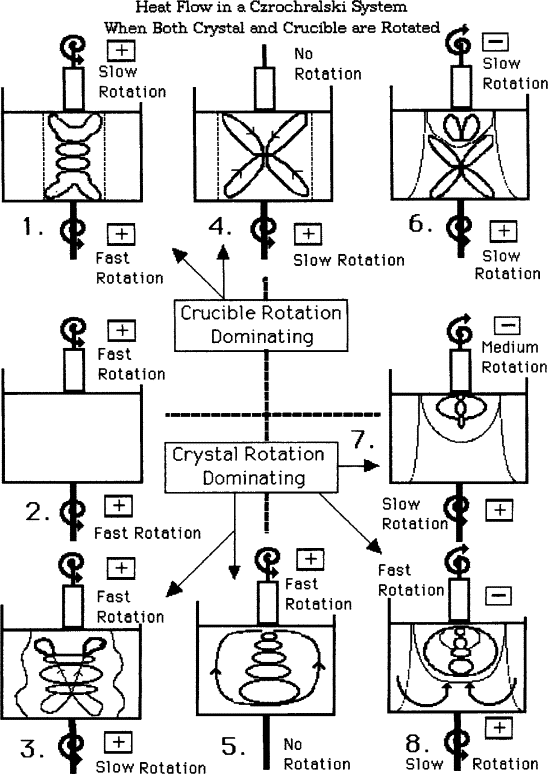
A seed crystal is lowered into the molten material and then is raised slowly, allowing the crystal to grow onto seed. Generally, the crystal is rotated slowly as it grows to provide a slight stirring of the melt and average out any temperature variations that would cause inhomogeneous solidification. This technique is widely used in growing Si, Ge and some of the compound semiconductors.
In pulling compounds such as GaAs from the melt, it is necessary to prevent volatile elements (e.g. As ) from vaporizing. In one method a layer of B2O3, which is dense and viscous when molten, floats on the surface of the molten GaAs to prevent As evaporation.This growth method is called liquid-encapsulated Czochralski(LEC) growth.
In Czochralski crystal growth, the shape of the ingot is determined by a combination of the tendency of the cross section to assume a polygonal shape due to the crystal structure and the influence of the surface tension, which encourages a circular cross section. The crystal facets are noticeable in the initial growth near the seed crystal. However, the cross-section of the large ingot is almost circular.
In the fabrication of Si ICs it is economical to use very large Si wafers, so that many IC chips can be made simultaneously. As a result, considerable research and development have gone into methods for growing very large Si crystals.
Type of Silicon Wafers
Type of Doping
Silicon wafer is doped with either n or p types. These are the two types of doping in silicon wafer.
Crystal orientation
It is mainly two types of crystal orientation,i.e. <111> and <100> (Miller Indices of plane)
Polished Side
Depending on the polished side, silicon wafer can be divided into two categories, i.e.
I. Single Side Polished (SSP) : In this type one side is polished mirror like, other side is opaque like.
II. Double Side Polished (DSP) : In this type both sides are polished mirror like.
Size of wafer
There are different sizes of wafers. Example : 1”, 2”, 3”, 4”, 6”, 8”
How to identify type of doping and crystal orientation
There are two different types of cut to distinguish different types,i.e. Primary cut and Secondary cut. Angle between primary and secondary cuts helps us to distinguish types.
If the angle is 0o , it is p type , <111> oriented. (i.e. single cut )
If the angle is 45o , it is n type , <111> oriented.
If the angle is 90o , it is p type , <100> oriented.
If the angle is 135o , it is n type , <100> oriented.
Here we’ll discuss mostly p <111> wafer , sometimes p <100>.
Mathematical Calculation:
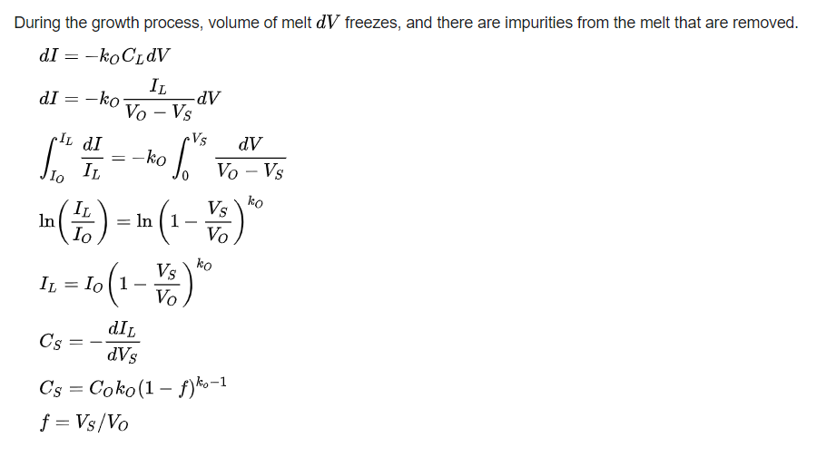
Concerning a mathematical expression of impurity incorporation from melt, consider the following.
The impurity concentration in the solid crystal that results from freezing an amount of volume can be obtained from consideration of the segregation coefficient.
Ko : Segregation Coefficient
Vo : Initial Volume
Io : Number of impurities
Co : Impurity concentration
VL : Volume of the melt
IL : Number of impurities in the melt
CL : Impurity concentration in the melt
VS : Volume of the solid
CS : Impurity concentration in the solid
Cleaning Process
Types of contaminations of wafer surface
There are two types of contaminations,such as
Inorganic / Metal ion pollutants
Organic pollutants
Cleaning of contaminations from wafer surface
Cleaning of Metal / inorganic pollutants
There are two types of cleaning,such as
RCA or base cleaning
Deionized water + NH4OH + H2O2 (5:1:1)
Piranha acid cleaning
H2O2 + H2SO4 (1:1 & 1:3) (Demonstrated in lab)
Cleaning of organic pollutants
Acetone cleaning : Deionized water + Acetone
Piranha Cleaning Process
Apparatus used
Quartz beaker and wafer holder 2. Teflon Tweezers 3. Nitrile Gloves
4. Borosil Glass beaker 5. Nitrogen gun 6. Desiccator
Chemical Used
98 % H2SO4
30% H2O2
1% buffer HF solution
Nitrogen gas
Deionised water (18.2 mega ohm-cm )
Procedure
Place the contaminated silicon wafers in the quartz holder and put into the quartz beaker.
Poured H2O2 first and then poured equal amount of H2SO4 to maintain the ratio 1 :1
Some points to be remembered here:
The order of mixing is not reversed to avoid exothermic explosion
In industry, the ration may differ, it could be 1 : 3
A huge amount of heat is evolved and bubbling is coming out which depicts the exothermic cleaning . Keep the solution about 45 minutes.
The wafer is rinsed with deionised ( DI ) water. The surface is now hydrophilic in nature due to the presence of a few nanometer thick native oxide layer.
The wafer again dripped into the 1% buffered HF solution to etch out the surface and remove the native layer which is not required.
Again silicon wafer is rinsed with deionised ( DI ) water, the surface is now totally hydrophobic. No water droplet is present on the surface.
This changes the visual interpretation of removal of native oxide.
The wafer is dried with help of N2 gas and stored in a vacuum desiccator to avoid any further contamination.
Piranha Process
H2SO4 + H2O2 → H2SO5 (Caro’s Acid ) + H2O
Thermal Oxidation Process
If silicon is exposed to an oxygen or air ambient. There is a chance to form a thin native oxide layer with .5 - 1nm on the surface rapidly. That oxide layer is not uniform and importantly not defect free. These two features are very vita for MOS cap. Device fabrication. That's why we have 1% buffer HF cleaning previously.
Silicon oxide is used to isolate one device from another, to act as gate oxide in MOS structures, and to serve as a structured mask against implant of dopant atoms. That silicon oxide layers can also be produced by deposition techniques, like chemical vapour deposition, sputtering etc.
Thermal oxidation is a complex process where a diffusion of oxidants. A chemical reaction and a volume increase occur simultaneously to convert the silicon substrate into oxide. This process is strongly influenced by the used oxidant species, the oxidant ambient with temperature and pressure, and also the crystal orientation of the substrate. With these parameters the quality and the growth of the oxide during the manufacturing process can be controlled.
The small dimensions and high performance of modern MOS devices require ultra thin silicon oxide layers for gate dielectrics. Apart from the exact thickness control, pure silicon oxide has some difficulties to fulfil all requirements at such thin thickness.
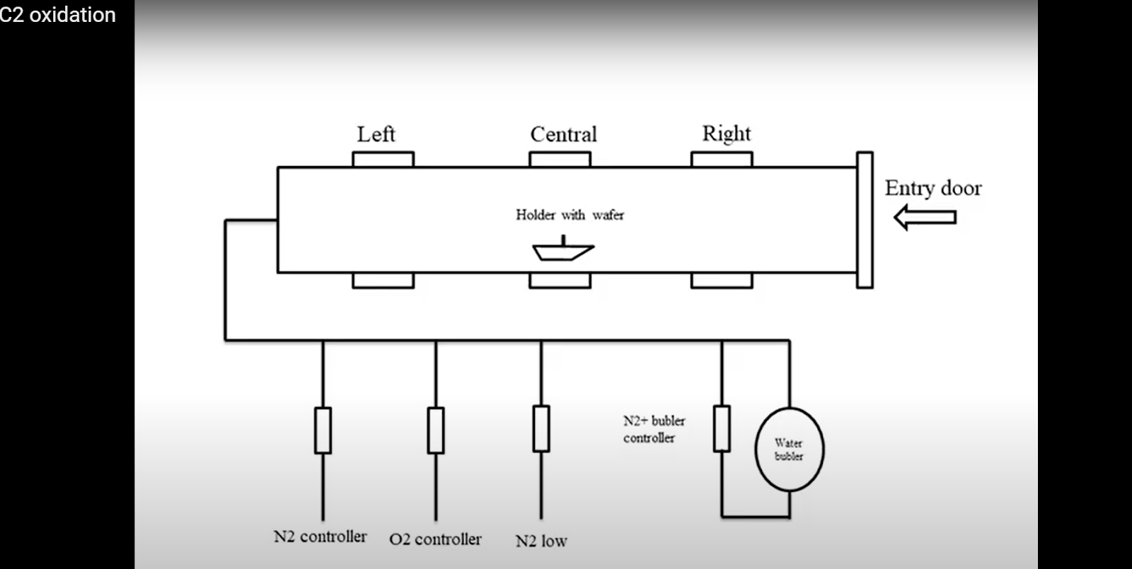
Thermal Oxidation Diffusion Furnace:
Three stack and three zone furnace
Entire diffusion chamber is made up of quartz
The quartz is segregated by three different temperature zones w.r.t. the position of heating coil.
Central zone, Right zone and Left zone. The quartz boat containing cleaned silicon wafer is placed in the central zone
The entire tube temperature is maintained using Gaussian distribution w.r.t. The three different coil temperatures
The quartz made apparatus is used to hold wafers and to close the lid of furnace at the entry point.
The entire chamber is maintained inert with the continuous flow of nitrogen gas into it.
Furnaces used for diffusion and thermal oxidation at LAAS technological facility in Toulouse, France.
For more details, you can visit Thermal oxidation .
Procedure
Insert the quartz holder with a wafer by the quartz rod, and close the lid with two opaque quartz supports to resist the heat dissipation.
Allow temperature rising to the set value at which the oxidation process is going on, here it is 1000o- 1200oC. The temperature ramp is 10oC/min. After the process, it will cool down.
The entire oxidation process is divided into three steps : Dry- Wet- Dry. The time allowed for these steps is 10 min - 5 min - 10 min. In the entire process the tube is maintained inert using the constant flow of nitrogen gas which is controlled by N2 controller.
After temperature is reached to the set value, for the first dry oxidation process the oxidation gas flow is allowed to inside of the tube with N2 flow with help of O2 controller.
In the next step, first wet oxidation process the water vapour form bubbler, allowed to the tube with N2 flow with help of N2 +bubbler controller.
After that, in the second dry oxidation process again the oxygen gas flow is allowed inside the tube with N2 flow with help of O 2 controller.
There are two intermediates in the entire process, at that time the N2 low controller is maintained the gas flow to control the inertness of the entire tube.
The amount of gas flow is controlled by the controller using the unit SLM (standard litre per minute).
The oxide growing pattern is top to down approach. After the first layer of oxide which is for dry oxidation, the next layer for wet oxidation is created below that previous layer not above.
Si + O2 → SiO2 (Dry oxidation)
Si + 2H2O → SiO2 + 2H2 (Wet oxidation)
Deal- Grove Model

The quality of oxide is defect free and uniform thickness in dry oxidation and it is slow in growth rate. But in the wet oxidation the quality is not good but the rate of growth is fast. This can help to increment the oxide thickness.
The oxide rate in <111> crystal orientation is faster than the <100> crystal orientation.
There is visual change in the wafer colour of presence of oxide. We are planning to grow 100 to 200 nm thick silicon oxide. Depending upon the oxide thickness the incident light gets diffracted and the colour change is noticed.
The ellipsometry technique is used to measure oxide thickness.
Metallization
Metallization is the process by which the components of IC’s are interconnected by a conductor. This process produces a thin film metal layer that will serve as the required conductor for the interconnection of the various components of the chip.
Another use of metallization is to produce metalized areas called bonding pads (;or contacts) around the periphery of the chip to produce metalized areas for the bonding of wire leads from the package to the chip.

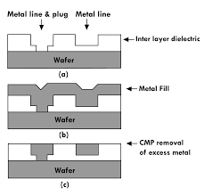
Types of Metallization
Physical Vapour Deposition (PVD)
Atoms / molecules (vapor) of the desired material are directly deposited on to the substrate from the vapor phase. PVD is a line of sight deposition technique, so that the substrate must be in front of the source. The material to be evaporated is heated and the atoms are then deposited on the substrate.
Thermal Evaporation
Electron Beam Evaporation
Sputtering
2. Chemical Vapour Deposition (CVD)
Use of a chemical reaction from a derivative of desired material which is to be deposited.
Metal used for Metallization
➢ Some metals films that are easily deposited by evaporation:
Aluminium, Copper, Chromium, Gold, Silver, Titanium, Palladium.
Aluminium
Aluminium (Al) is the most commonly used material for the metallization of most IC’s, discrete diodes and transistors. The film thickness is about 1 micrometers and conductor widths of about 2 to 25 micrometers are commonly used.
➢ Advantages
It has relatively good conductivity.
It is easy to deposit by vacuum evaporation (melting point ~600oC).
It has good adherence to the silicon dioxide surface.
Aluminium forms low resistance, non rectifying(i.e. ohmic) contacts.
It can be applied and patterned with a single deposition and etching process.
➢ Limitations
It can not withstand high temperature (more than 600oC) operation.
Aluminium suffers from electromigration.
Thermal Evaporation
➢ Steps involved in the process
Converting the condensed phase (generally a solid) into gaseous or vapour phase.
Transportation of the gaseous phase from the source to the substrate.
Condensation of the gaseous source on the substrate.
The whole process is done in vacuum chambers. A mechanical pump (rotary) can reduce the pressure to about 10-3 mbar. An oil diffusion pump can bring the pressure down to 10-5 mbar and with the help of a liquid nitrogen trap as low as 10-6 mbar.
➢ Need of Vacuum
To reduce the particle density (impurities)
To remove the gas/ air molecules.
To reduce the thermal transport to substrate.
Less current required to achieve desired filament temperature.
To increase the mean free path (average distance between two successive collisions)


***Picture courtesy : Internet
Comments